@pygmalion Sure mate. I'll just go check the specs on the digital pot. The circuit voltages in the gain circuit aren't that high anyway, even "line" voltage [CD players, tape decks etc.] is only 1V p-to-p, mic is considerably less.
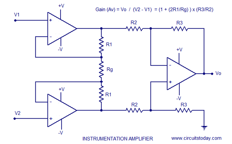
I'm leery of fiddling with the THAT1512 as it's an instrumentation amp which is essentially three or four op-amps wired like this:
THAT obviously make the whole thing on a monolithic piece of silicon, but that's (THAT's 🤣 ) what it is.
One tick and I'll draw you up something that should do the job.
Take everything I say with a pinch of salt, I might be wrong and it's a very *expensive* way to learn!
@axy_david I designed this as a custom pcb in kicad, do you want the gerber file? (I am new to pcb's not sure the best way to share it.)
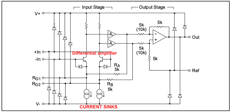
Here's the guts of the THAT1512 -
You can see on the input stage there are a couple of constant current sinks that set the drive current for the differential front end formed by those two NPN transistors.
This is all signal path stuff - the voltages here are relatively small since the gain resistor is connected to the emitter side. Any large voltages are generated dropped across the collector of each input transistor. It's not clear how much since we don't know the value of the resistors or the magnitude of the current sink.
But these are essentially emitter followers - that means the voltage at each emitter "follows" the voltage at the base (minus about 0.7 volts). https://en.wikipedia.org/wiki/Common_collector
Rg is in that part of the circuit so it can be controlled dynamically.
You can check the voltage when your circuit is powered by measuring the DC voltage drop across Rg. I'd be surprised if it even registers because it's connected between the emitters of what is (in essence) a long-tailed pair.
https://en.wikipedia.org/wiki/Differential_amplifier
Unfortunately, Wikipedia's editors like to look smart so they tend to overcomplicate these pages with all sorts of math that's not really helpful if you just want to understand the basics!
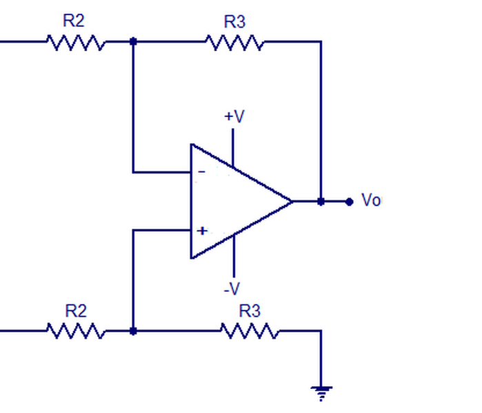
All Op Amp have a circuit similar to this - the two bases of the LTP (differential amp) are connected to + and - in respectively. You CAN make a poor man's diff amp similar to the THAT1512 like this:
But without really *really* expensive resistors you won't get the high CMMR (common mode rejection) - that is NOISE rejection that the THAT will offer.
This (incidentally) is one area where Matt's design falls over. The THAT is driven by a FET differential amplifier but the source impedance that the THAT sees is determined by drain impedance and the source impedance BUT those resistors are only good for DC, the actual impedance when this circuit is operating means there is a considerable difference in impedance which effects the load the two inputs see and that screws up all the benefit of the THAT1512!
The source impedance from each FET terminal loads what you can see as R2 in the highly simplified version. And (if you bother to do the maths, I wouldn't, you can take it as read) you'll understand that the R2s are in parallel with the source impedances presented by the FET and since they are not the same, the actual load varies. Remember that just because two resistors are equal in something like a phase splitter, particularly a FET one, the actual impedance is vastly different.
The proper way around this is to put emitter followers on each phase and drop the output impedance down to a few ohms which is predicted by the properties of the two transistors and that's WAY closer to what the THAT sees right now.
This is what Schopes did with their circuit back in the 1960s but I'm going way off track here.
SOOOOOO...
I would predict that you can put the digital pot in the Rg position but clearly, make sure I haven't missed something first! I'll check the data sheet in a mo to see how much voltage the resistor ladder can tolerate, it's possible it might be able to take more than the Vcc - but I haven't checked as yet!
But here's where that falls down. Rg is in the differential emitter circuit, which means ANY noise generated there is going right back into this highly sensitive network and will be amplified accordingly. For this reason, it's usual to put a gain control (volume knob) later in the circuit when most of the gain has been taken care of an a small amount of noise is going to be swamped by the signal.
That does mean adding in another op amp, I'd suggest the NE5532 (good quality bipolar for audio applications), but a current hog so no good for batteries or if your current is limited. If it is, something like the TL072 is better.
Either way, the circuit is pretty simple. I'll just take half-an-hour to do that and I'll be right back with you!
QUICKIE EDIT:
https://www.thatcorp.com/datashts/dn138.pdf
This application not from THAT shows what you're trying to do (but with a fixed pot of course). Given that THAT has specified 10v for the capacitor though, it's definitely worth checking the voltage drop across Rg in Matt's design to make sure I haven't dropped a 0 somewhere!
Take everything I say with a pinch of salt, I might be wrong and it's a very *expensive* way to learn!
@theguy This is possible but not with the circuit presented here. I'm working on something suitable right now, but you might not get this in time?
Take everything I say with a pinch of salt, I might be wrong and it's a very *expensive* way to learn!
SOOOOOO...
I would predict that you can put the digital pot in the Rg position but clearly, make sure I haven't missed something first! I'll check the data sheet in a mo to see how much voltage the resistor ladder can tolerate, it's possible it might be able to take more than the Vcc - but I haven't checked as yet!
But here's where that falls down. Rg is in the differential emitter circuit, which means ANY noise generated there is going right back into this highly sensitive network and will be amplified accordingly. For this reason, it's usual to put a gain control (volume knob) later in the circuit when most of the gain has been taken care of an a small amount of noise is going to be swamped by the signal.
That does mean adding in another op amp, I'd suggest the NE5532 (good quality bipolar for audio applications), but a current hog so no good for batteries or if your current is limited. If it is, something like the TL072 is better.
Either way, the circuit is pretty simple. I'll just take half-an-hour to do that and I'll be right back with you!
QUICKIE EDIT:
https://www.thatcorp.com/datashts/dn138.pdf
This application not from THAT shows what you're trying to do (but with a fixed pot of course). Given that THAT has specified 10v for the capacitor though, it's definitely worth checking the voltage drop across Rg in Matt's design to make sure I haven't dropped a 0 somewhere!
In the document you provided, there is a capacitor in series with the potentiometer - something not present in Matt's circuit. I do not understand what else is wrong with Matt's circuit, because I did not quite understand your explanation.
You also say that it would be good to put another amplifier between the preamp and Matt's amplifier. Why don't we keep all these corrections as simple as possible - I do not feel like doing everything from scratch.
So if I understand you correctly, you mean I could connect the digital potentiometer directly to the THAT1512, but should check with a voltmeter first? I could do that, but the voltmeter will not detect high frequency components.
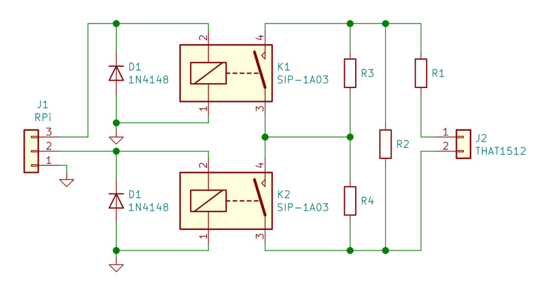
Finally, this is the circuit I wanted to make to have four different gains controlled digitally from the Raspberry Pi. Pretty simple, I can do it in a few minutes (after getting all the parts from China.
Ah, that's a bind (but not surprising). The ladder in the MCP41XXX series is limited to Vdd.
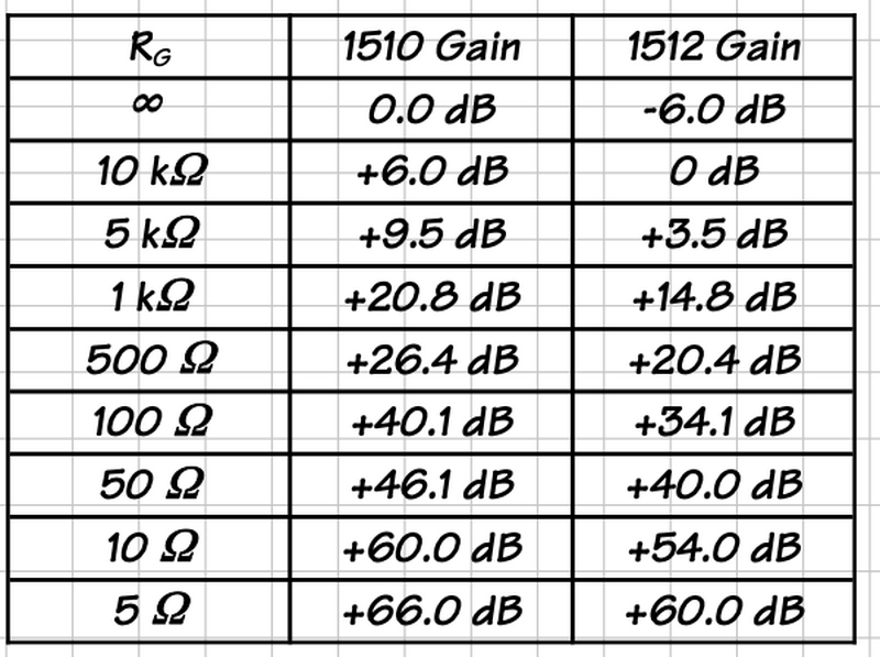
Here's the gain levels from THAT - which suggests Matt's aiming for around 60 dBs of gain (Rg = 5R1).
60 dB is a voltage gain of x 1000
So 1 mV p-to-p in = 1 V p-to-p out - nice and simple so far!
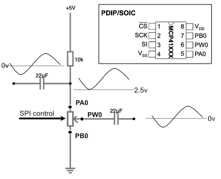
The gotcha for digital pots though - is that circuit is A/C so it's actually swinging from +0.5 to -0.5 which is less than ideal, but you get around that one by biasing it with a resistive divider after the decoupling capacitor. This means between the circuit from the output of the THAT1512 after the 22u capacitor.
The value of Rg is best fixed at 5R so you get full swing from the THAT1512 but remember you're also driving a USB C input but using a USB 2 standard (with the ADC that Matt has used). That means the ADC chip is subject to precisely the same input voltage swing problems as the MCP41xxx digital pot, 5 V in other words so if this circuit doesn't blow the digitiser (although it might have limiting diodes) but you'd hear that as clipping.
In fact, you could probably do something like this - my simulator doesn't have a symbol for this but this should make some sense. We just give the small signal from the THAT1512 a kick to 2.5v (raising the ground floor to 2.5 V) and then convert it back to AC via a cap into the USB ADC.
It's easier than fiddling with the gain control on the THAT1512. Let me know if that's not clear mate.
Take everything I say with a pinch of salt, I might be wrong and it's a very *expensive* way to learn!
So 1 mV p-to-p in = 1 V p-to-p out - nice and simple so far!
The gotcha for digital pots though - is that circuit is A/C so it's actually swinging from +0.5 to -0.5 which is less than ideal, but you get around that one by biasing it with a resistive divider after the decoupling capacitor. This means between the circuit from the output of the THAT1512 after the 22u capacitor.
The value of Rg is best fixed at 5R so you get full swing from the THAT1512 but remember you're also driving a USB C input but using a USB 2 standard (with the ADC that Matt has used). That means the ADC chip is subject to precisely the same input voltage swing problems as the MCP41xxx digital pot, 5 V in other words so if this circuit doesn't blow the digitiser (although it might have limiting diodes) but you'd hear that as clipping.
In fact, you could probably do something like this - my simulator doesn't have a symbol for this but this should make some sense. We just give the small signal from the THAT1512 a kick to 2.5v (raising the ground floor to 2.5 V) and then convert it back to AC via a cap into the USB ADC.
It's easier than fiddling with the gain control on the THAT1512. Let me know if that's not clear mate.
Regarding the USB input - are you talking about an audio card when you mention the ADC chip? I would guess that the audio card should be designed to withstand a sustain reasonable input DC bias. After all, you never know what the user will connect the audio card's input to.
I will resume everything to make sure I have understood you correctly.
- As THAT1512 instructions suggest, RG should be in series with a capacitor so that RG only acts on AC voltage.
- If we assume that the input voltage oscillation is much smaller than 5V, we can simply set the DC bias voltage of the digital potentiometer somewhere between 0V and 5V and the AC voltage oscillations around this DC bias voltage will not go below 0V and above 5V.
Maybe it would be a good idea to put 10k resistor between the digital potentiometer and the ground too, because at the maximum value of the potentiometer the AC voltage will oscillate around 0V. This way DC bias will be between 1.67V and 3.33V.
EDIT: I just realised that your solution, although interesting and worth trying, does not work at low frequencies. Because of the reactance of the capacitor... Z = 1/(2 pi f C) gives about 500 Ω for each capacitor. 🙁
@marcdraco thanks for the insight I admit I'm tempted to go a little more, maybe playing around with a bigger diaphragm honestly, but is there any point? That Neumann U87 Ai sounded somewhat better, especially in the lower mids and low frequencies, but is it really feasible to get closer to a more neutral response? Especially without over-complicating the circuit?
I'm definitely looking for a donor body and most likely will just buy some second hand cheap crap for the body, because I'm planning to make another one, this one got my feet wet with the mic design possibilities.
@lmarzen Also thanks for your posts man, it really helped me troubleshoot when I had some issues with the resistance for the amplification.
It would be nice with the gerber file, even better with :
example.kicad_pro, example.kicad_sch & example.kicad_pcb
I would like to do some modification for it before printing it, although even as is is good enough, I'd rather have it one sided.
@axy_david Glad my post helped! I created a github repo for my pcb design. https://github.com/lmarzen/diy-microphone
@axy_david The MX900 is a nice little donor body that you should be able to find used for about £30-60 depending on where you look. It's tighter (oh er missus) than the ludicrously cheap Neewer NW800 but the construction and component quality far exceeds it. What lets it down is (again) a cheapish capsule although I'm not 100% sure which one it is until I open mine up.
Take everything I say with a pinch of salt, I might be wrong and it's a very *expensive* way to learn!
@pygmalion I agree that the device we're connecting to SHOULD have DC blocking but I tend to be overcautious when I don't know what I'm driving. We don't even know the input impedance but it's fair to assume that it's quite large.
I'm a little confused by your calculations though. This is what I get:
The source impedance as seen by the output pin of the 1512 (input into this circuit) equals two 10K resistors in parallel which is 5 K.
The "wiper" (PW0) picks a developed voltage of at any given point but the load seen from the THAT1512 is always just 5 K. This never changes although it IS loaded slightly by the following stage. I'm assuming that it's of sufficiently high impedance not worry about. I'd probably double check with a voltmeter just to make sure no bias voltage is appearing at the input, just to be safe.
OK, so the -3 dB point is given by 1/(2*pi * r * c)
= 1/ (6.28 * 5 e3 * 2.2 e-6)
= 1/ (6.28 * 5000 * 0.0000022)
= 14Hz (give or take)
You don't have to fiddle with all these numbers though, the magic of the Internet gives us sites like this:
http://www.learningaboutelectronics.com/Articles/High-pass-filter-calculator.php
If this is confusing (and bloody hell it wrapped me in knots the first time I saw one) you can think of a filter as being a voltage divider.
RC High-pass filters always start with a capacitor (because we're blocking infinitely low frequency down to DC) and low-pass filters always start with a resistor.
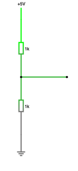
So the absolute simplest voltage divider looks like this. With two equal resistance values you just half the supply voltage.
The centre tap in this example is sitting at 2.5 volts but it's not very "stiff" (oo er misses) because anything connected from the tap to the ground "loads" the bottom resistor. That's why you don't see circuits like this used to split a power rail. It's not that they don't work, it's that they are mind-bogglingly inefficient.
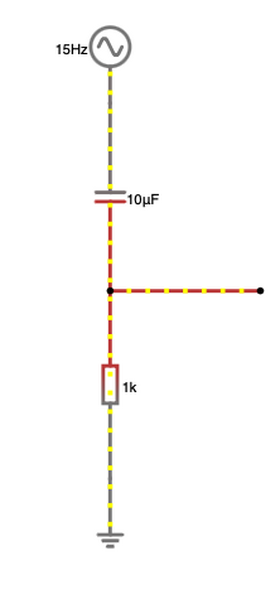
Ok, so let's look at at high-pass filter arranged like this ladder.
The reactance (X) of the 10 uF cap is (give or take) 1K at 15 Hz. which means a sine wave at this frequency is divided into two just as in the resistive divider above. This doesn't account for phase shifts, but we don't need to worry about those here.
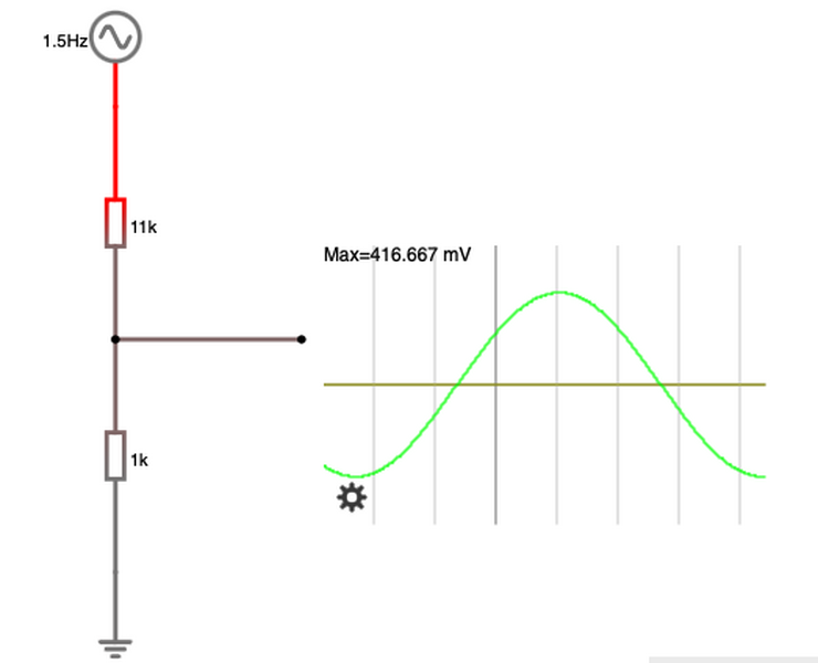
If we drop the f in to say 1.5 Hz, the reactance of the capacitor rises to around about 11K which produces a resistive ladder that looks like this:
The 11 k resistor I've shown here represents the reactance of the capacitor and you can see that the peak voltage is only 416 mV - 832 mV peak to peak. So if the AC (this example is at 5 V peak so 10 V full swing.
That gives us an attenuation of:
0.832 / 10 =
0.0832
(Guess that doesn't take a genius to work out - but I used a calculator so that tells you all you need to know):
To get the dB (peak-to-peak) attenuation we do:
20 * log(0.0832)
= -21 dB
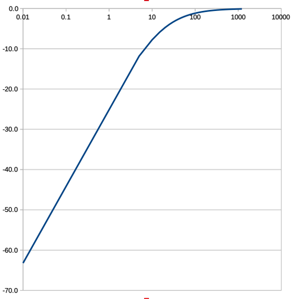
For my own curiosity I did a quick spreadsheet with all the various operations including the current at a given frequency and the voltage drops across the resistor and capacitor. It charts like this with frequency increasing on a LOG scale across the top and dB of gain down the left.
I can't share the spreadsheet here but if you wanted it I'm sure we can find a way.
Take everything I say with a pinch of salt, I might be wrong and it's a very *expensive* way to learn!
@marcdraco thanks for the insight I admit I'm tempted to go a little more, maybe playing around with a bigger diaphragm honestly, but is there any point? That Neumann U87 Ai sounded somewhat better, especially in the lower mids and low frequencies, but is it really feasible to get closer to a more neutral response? Especially without over-complicating the circuit?
I'm definitely looking for a donor body and most likely will just buy some second-hand cheap crap for the body, because I'm planning to make another one, this one got my feet wet with the mic design possibilities.
Those Neuman capsules can run you a lot of money and the circuits presented here just won't do them justice. You absolutely HAVE to use more complex designs - some of which are above my pay grade! But the OPA Alice is just a flat output using a dual JFET (actually a BiFET) op-amp of very high quality indeed. And even then, you still need to plug that into a balanced pre-amp - which is what the THAT1512 does in Matt's version.
This is the OPA Alice "head" which delivers a mic-level input of about 1mV out at very-low impedance to drive a 600 ohm load.
There are a couple of things to note though, mainly that the capsules themselves are known to have a non-flat frequency response which is part of what makes them so pleasant for micing all sorts of things from percussion to vocals. As I recall there's a little bit of lift above 6 KHz.
Thing is, recording is creative, we don't actually *want* a flat response unless we're building some sort of specialist microphone for scientific work.
It's that non-flat response with a slight lift in the presence (4-6 KHz but that depends who you talk to) is what gives these devices a pleasant sound. It's rather like doing a portrait - you show someone exactly what they look like and it's not flattering, so we tinker around with the settings to adjust colour and such so it's more flattering.
Mics are no different!
Take everything I say with a pinch of salt, I might be wrong and it's a very *expensive* way to learn!
@marcdraco That's a very interesting way to put it.
For me since I produced music for 12 years I like flat responses since I take it's easier to work with it, like eqing or using compression on it. But you do make an interesting point. I heard about those OPA alice, is that the pimped version?
Do you know of some capsules that are reasonably priced that could give a nice low and mids like the Neuman?
And if so would it be possible to combine the alice with the THAT1512 and make a sort of a hybrid?
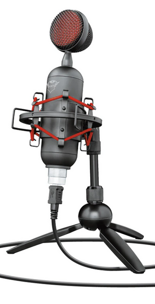
In the end i ended up with a trust buzz, it looks...interesting has USB B Port and was around 20 eur new, which is cheap.
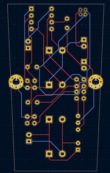
Here is my modified version of the @lmarzen board, initially I wanted it one sided but I think it would complicate the design too much. So i chose to simplify the existing version focusing on using as little material as possible. Feedback would be greatly appreciated since I rarely dabble into PCB design.
Oh that's pretty! @axy_david I'm actually making a "hack" version of something that looks a little like that. I just don't have our host's skills, charm, good looks... (Damn him. LOL.)
From what I've seen of Neumann K47 clones like this they all have the colouration. Not eyewatering money, but it is out of my budget.
https://microphone-parts.com/products/rk47-microphone-capsule
You will more likely get a flat response from an SDC like the Primos and many of those have an internal FET so there's less fiddling around.
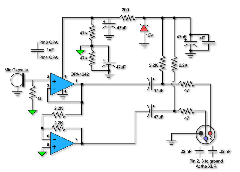
OK, so let's look at OPA Alice and what it does.
The circuit is actually a lot simpler than it looks, but I'll break it down a bit.
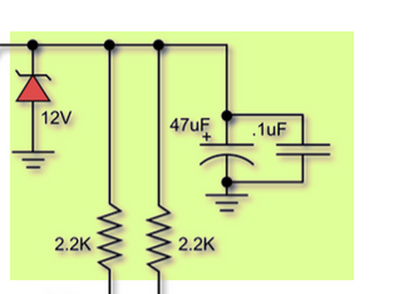
Let's start with the power supply. This takes the two P48 (48 V) power rails (which are each connected to 6.8K series resistor already) combines it into a single feed and pops it into a 12V zener.
Note that the bottom half of the zener is connected to P48 ground reference (0 V) or screen - this will become relevant in a moment. The 48uF and 100nF in parallel seem a bit barmy but this is where low ESR capacitors come in. The 100nF is there to catch any HF noise on the line - likely the horrible scream that comes from Zeners when they avalanche, which is how they work.
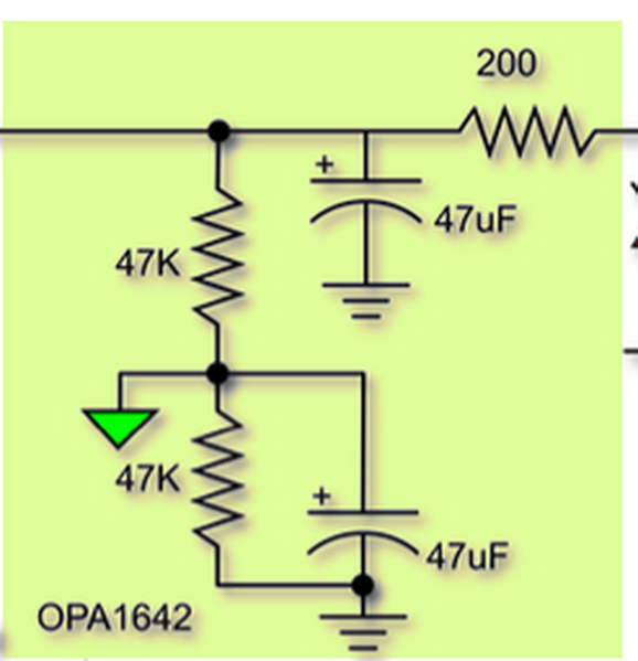
Ok next little section takes the filtered 12v and filters it a little more through the 200R and 47uF but then there's a clever bit to bias the op amps. See how the circuit passes into a pair of 47K resistors bypassed but their own 47uF capacitor.
The clever bit is that green ground. It's isolated from the main ground and delivers a ground "reference" at half supply. This allows the op amp to run on a single supply that appears to be +6V & -6V as far as the device is concerned. This is similar to what I did for Pygmalion's electronic volume control.
Now let's look at the balanced line drive. This is what the JFET does in Matt's version of the Alice circuit - and it's wrong because the impedances don't match (even if the DC resistance at the source and drain matches) - the properties of the JFET send that all do-lally.
The idea is to split the phase of the microphone capsule and deliver it to a balanced preamp. Crucially (and even surprising to me) the mic signal input expects just 1mV into 600 ohms. Such a low impedance means you need the current to be able to carry a fiddling 1000th of a volt at currents of up to around 10 thousandths of an amp! It's a wonder it works at all!
The 600 ohm is a PITA but it comes from the telephony days and it's stuck
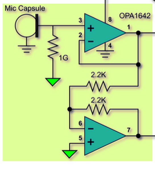
This is how the Alice does it:
What you have here is a voltage follower (which is matching the impedance because the OPA1642 is has JFET inputs.) The 1 GIGA ohm input impedance catches all of that lovely signal coming from the capsule. Note the ground reference point is different.
I only have 1M to hand so mine do lose some signal at that stage alone. A very high-quality resistor is required here as noise is a factor and thermal noise increases with the resistance.
A follower is the simplest op amp circuit of all. I'll only look at what it does, not how it works.
The signal at pin 2 (non-inverting) appears at pin 1 and is immediately fed back to pin 3 (inverting). Although the amp has an open loop gain of millions (or billions, more is better) and every bit of that signal is returned to the inverting input, immediately cancelling out 100% of the gain.
Which sounds barmy if you've never met this circuit before but you've seen me talk of emitter followers perhaps? This is like an emitter follower from the DC universe. 🙂
The voltage at pin 1 FOLLOWS (is a replica of) the voltage at pin 2 but rather than having an impedance of 1 G, it's a fraction of an ohm. So driving just about anything is possible so long as there is sufficient current (remember P48 is limited to about 15mA).
That output is now split off:
One goes to pin 2 on the XLR ("hot" or in phase) via a 47 uF DC blocking capacitor and 47 ohm resistor which sets the output impedance.
The other goes to the inverting input of the second op amp via a 2K2 resistor.
This is a weird looking configuration but it forms a x1 inverting amplifier with an input impedance of 2K2. It's an inverting follower in other words and the output at pin 7 is delivered to the "cold" pin on the XLR using precisely the same configuration as before. Since the output of each op amp is almost 0, the output impedance as seen by the balanced cable is the same too. This is absolutely crucial to get every ounce of signal into the pre-amplifier. It even affects the noise levels to some degree.
But note how pin 5 is taken to that "fake" ground formed earlier. This DC path biases BOTH amplifiers at the same time by pushing the 0V reference to 6V more positive than the circuit ground.
You should note that the "virtual" ground is shared only between a few points to make sure the AC signal path is biased correctly and there's no clipping.
When the signal arrives at the other end - a THAT1512 here the "cold" is inverted again and the result is added to the "hot" signal.
But note that any noise and crud is received by both signal lines equally (this is why the impedances need to match). When you flip the "cold" signal back into phase with the "hot" one - the noise also gets inverted. When the two signals are summed, the noise gets cancelled out.
Dang clever.
Take everything I say with a pinch of salt, I might be wrong and it's a very *expensive* way to learn!
Here is my modified version of the @lmarzen board, initially I wanted it one-sided but I think it would complicate the design too much. So i chose to simplify the existing version focusing on using as little material as possible. Feedback would be greatly appreciated since I rarely dabble into PCB design.
Sorry, long post meant I was replying to your mic being pretty David.
Only thing that comes immediately to mind is you haven't "painted" a ground plane. KiCAD will do that for you automatically. It can make a big difference in shielding everything even from the power signals. A large area gives the energy a place to flow. (We used to think electrons moved through wires, turns out all that was wrong... it's all done in waves...)
Also it looks like you're using the same width for signal and power "rails". This is where strip board falls down. Anything carrying power (particularly where noise is a problem) should be nice and wide (within reason). It's not that we're worrying about current, it's the track impedance that can start having an effect at these signal levels.
Decoupling capacitors (I can't see what you have and where) should always be as close as possible to the thing they are decoupling to reduce the effect of lead inductance. (Yeah, there's another one they don't tell you in physics class!)
I'd have to look at the full KiCAD files to see if there's anything else but it looks competent for someone with little experience.
Don't worry about being double-sided: nothing wrong with that but there are issues with the layout that might not be obvious. I'm "OK" at this so I'll give you some pointers if you drop me the files, but I can point you to a couple of YouTubers who are absolutely out of this world.
I'll take it slower than they do though.
Take everything I say with a pinch of salt, I might be wrong and it's a very *expensive* way to learn!
@marcdraco https://github.com/axydavid/diy-microphone
This is my fork
@axy_david I'm just fighting with my Mac to see how well the "TL0 Perks" works.
That's my take on this thing that delivers audio directly to USB with fewer components. I'll put a board up as soon as I've done testing it to make sure it actually works as advertised!
Your work looks really good! So you got the whole thing inside the Neewer donor body? Sweet!
Take everything I say with a pinch of salt, I might be wrong and it's a very *expensive* way to learn!
@marcdraco I just modified @lmarzen diagram however i did not modify the component placements, just the paths so it should still fit in.
@axy_david Still, nice job overall.
I'm still working on getting a USB-powered circuit together that doesn't rely on such a complex design. Not that I'm particularly fond of USB digitisers (which reminds me, I need to order one..) but if that's what people want... However, see my note at the bottom of this post and you're in for a nasty surprise!
There are a few bits to consider
Impedance matcher - while a 1G resistor is preferable, bootstrapping might deal with that for lower values.
The output from the buffer (impedance match) is just a few hundred ohms at most (probably a lot less) so that can drive any GP op-amp or even a high-performance such as the OPA 164x series. You can get those as a single (OPA 1641) but they do seem pricey. There are plenty more that are just as suitable because once you've used the FET, you don't need an op amp with a JFET input. Nothing saying you *can't* use one but it opens the possibility for a world of different options. On paper the TL07xH (the updated version of the TL07x line) look really nice but that's just one I looked at.
But here's where you need to hold onto your hat a little.
I expect the digitiser is expecting line level (consumer) which is 1V p-to-p. Microphones typically output about 1mV max which means you need 1000x gain!
This is where the real design choices lie.
Noise figures are quoted as 1/root Hz which is damn confusing but it's because they're using a Poisson analysis. You take the square root of your operating bandwidth (20-20,000) and that gives you the noise you can expect. So you can take a rough guess at the total noise figure as being the specified amount (say 10nV for an OP071) and multiply that by 141. Giving a total noise figure of 1410nV (1.4 microvolts) which is around 700x lower than we can expect from the capsule.
But that has to be amplified by 1000 bringing it to 1.4 millivolts but that's drowned out by the capsule by a factor of 700 to 1.
The THAT1512 has an input noise voltage of 34nV at 0 dB dropping to about 1nV at 1000x (60dB) gain. It's not clear from the data sheets if the same can be said for the OPA07 however, TI does have some good notes on PCB design (see section 12 if you're interested). This is a bit over my level of education because I probably snoozed during those classes.
https://www.ti.com/lit/ds/symlink/op07c.pdf
I haven't built Matt's circuit myself since it was a bit out of my price range. The Murata inverter is a great choice but not really necessary since this circuit can (and should) be single-rail power. The inverter can also create a LOT of noise although the manufacturer claims it is magnetically sealed (it would have to be as this uses inductors and capacitors - thus producing tonnes of electrical noise. These frequencies are outside of the audio range but they do fold back into the audible spectrum, particularly if the line isn't sufficiently isolated. Think ground planes and see that note from Texas Instruments.
But then we come to the audio interface and it all goes wrong!
This isn't remotely HiFi with a maximum sample rate of just 48 KHz, it's actually rather ordinary ADC and the quantisation noise this thing is going to produce will outweigh any advantages of a decent capsule and amplifier.
Admittedly, I hadn't looked at this bit before (and I should have) since that's an essential part of the signal path. It's like putting a rocket engine into a soap-box go-kart. For that omission, I shall now spend the next hour sat on a bed of nails while the cat attempts to pick fleas from my head.
I'll see if I can find a better solution in the meantime. With such a choice, any gains we make at the head of the signal chain are swamped by the USB interface and that's a real shame!
I've done a quick bit of Googling and found that I have (somewhere) a USB sound card that has a microphone input - they sell for about £3 quid and while the quality is likely to be "ow, my ears are bleeding" I suspect they are quite usable and with such a thing, you don't need a whole bunch of supporting electronics - even the mic amplifier comes on the board, so you only "need" mic level of 1 mV. In theory anyway... 🙂
I'll find a cheap capsule later and see how good it sounds and then see about hooking up a buffered capsule like the JLI2555 to see what we can get out of it. If anything!
Take everything I say with a pinch of salt, I might be wrong and it's a very *expensive* way to learn!
@marcdraco are you implying that the usb interface is bad? I mean I doubt any significant audible differences could be heard at sampling higher than 48KHz.
Tho I will admit that I could not hear a significant difference between the 20 eur mic and this usbC one, only perhaps the fact that this one is more sensitive to sound, or perhaps gain, but the way it actually sounds, I couldn't hear any significant difference...
That being said the whole point of me making this mic is to have something portable so it's easy to carry and set up while having a great sound quality. However I do feel a little frustrated when a cheap mic that costs around 20 euros sounds similar to the one I spent 3 times the amount and built myself....
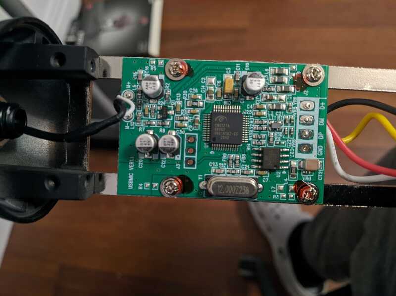
Nevertheless opening up this 20euro trust mic reveals that it actually has some decent components inside, have a look:
@diyperks Hi Matthew, I was just wondering if you sell these mics?
really interested in this, most beautiful design ive ever seen.
@axy_david Crazy isn't it? 🤯 I mean the price we pay for what looks like a pretty decent design. I don't have that one so I can't say what the capsule is. It's very likely an electret with an internal FET though (they're cheaper and can be made to look like a LDC).
16 bit integer, 48Khz is hardly studio quality - but it's perfectly acceptable for (say) digital radio or even MP3. This is why I've been banging on about this thing over many posts and now I find something utterly crap at the end of the signal chain. LOL.
If you really want spiffing (cough) expensive (cough) quality you're going to need something capable of 32bit floats at 192 Ksps which, I would expect is going to run you serious money. Probably won't work over USB 2.0 either due to bandwidth limits (I haven't done the math but I suspect you're into USB C territory there or even a PCI bus card which you need a desktop PC for.
But the point here is with something like that doing the conversion you're simply throwing money down the pan since Matt has specified some pretty high-grade components right up to that point.
To this end, I'm redoing the electronics with something more suitable (and cost-effective) with fewer components. The sim suggests (and it's a SIM remember) that just a simple JFET and a single transistor should be able to pump out sufficient voltage at a sufficiently low impedance to drive a mic input.
This grim-looking mess (sorry) is what I'm going to try first. Should be interesting to see if it works as advertised - I have done it once before but I made a bit of a pig's ear of the board so I'm going to have another crack and see if it really does work as advertised and then solder it to one of those cheap boards to see if I can make a poor-man's version. The really poor man's version would use a small (but quality) Primo capsule with internal FET. They're very good indeed actually and that saves a lot of harassment because they only need a single (load) resistor, a capacitor to block the bypass at 1.5-5 V supply.
Take everything I say with a pinch of salt, I might be wrong and it's a very *expensive* way to learn!
@marcdraco
Thank you for all your insights. I barely got past my circuits classes so I'm looking forward to seeing how your simpler design progresses. I was just about to order parts but I might hold off if there's a V2 in the works, I have no shortage of other projects. About the capacitors though: If a 2u2 film capacitor is used instead of a 22u electrolytic, does that change the value of the 2200u electrolytics in the diagram? My intuition is it wouldn't but I'm far too rusty to trust myself with this sort of thing and actually do the math (not to mention the non-linear components, which scare me immensely).
And about USB signals: ADC's are expensive but besides that the digital signal is fairly tame. The math for an uncompressed 32 bit PCM signal at 192khz looks like this:
(32 bits/sample)x(192x10^3 samples/second) = (6144000 bits/second)
Despite my preference for kibi/mibi/gibi (x1024 increments), the Wikipedia page for the USB protocol uses kilo, mega, and giga (x1000) so we'll stick with that (it makes the math easier anyways). We end up with a whopping 6.144 megabits per second. For reference (Wikipedia again), USB 1.1 can do almost double that, USB 2.0 reaches 480 mbps megabits, and the newest USB 4 can reach 80 gbps (that's over 13,000 uncompressed 32 bit 192khz signals). In short, computers are insane and I still underestimate them daily no matter how much exposure to them I get.
@marcdraco i mean the main way we listen to music is youtube or spotify, which both use some kind of compression on the audio, even me I use 48 kHz on my projects since I know once I export my music and upload it I will have to abide by these limits whenever I like it or not. So can you really make a case for anything higher than 48 kHz? Since it will be resampled down to it one you upload the music on a streaming site?
That being said you were right in your assumption, I wasn't able to find any 192Khz card on usb, however I did manage to find
24-Bit 96Khz ones on usb 2. However it's only on the output, the input is 24bit 48kHz
@axy_david Certainly better but as we've already agreed, USB really isn't the way to full studio performance. @ttamttam has done some figures but my guess is that studio digitisers take balance lines and do the ADC on board with some exotic stuff from Burr-Brown, Analog Devices or one of that bunch.
I think we're better off concentrating on the head of the signal chain and letting the USB ADCs look after themselves. Right now, a reasonable pre-charged (electret) capsule seems to offer the best value in terms of cost versus performance. When you start to get into "true" condenser microphone capsules you need to apply a bias voltage upwards of 30 V and often as high as 90 V. The p48 is ideal for this assuming it's suf
Although I've got pure transistor models working in simulation and on the bench, there's one I desperately want to try but I think I busted my last TL072 so I'm waiting on the order coming in.
It appears, and I could be mistaken, that the diaphragm only generates an alternating DC signal referenced to ground. I can do this as a thought experiment but without being able to test it...
I'm also looking at using diodes in place of the 1G resistor. Diodes are non-linear devices as you're probably aware but they can be biased by a bootstrap. Doug Ford (formerly Rode Microphones) found a device with the diodes on the JFET die for this exact purpose but I'm wondering if discrete diodes would be good enough. It's one of those things that can't hurt to try, especially as that 1G resistor is expensive as a through-leaded part.
Take everything I say with a pinch of salt, I might be wrong and it's a very *expensive* way to learn!
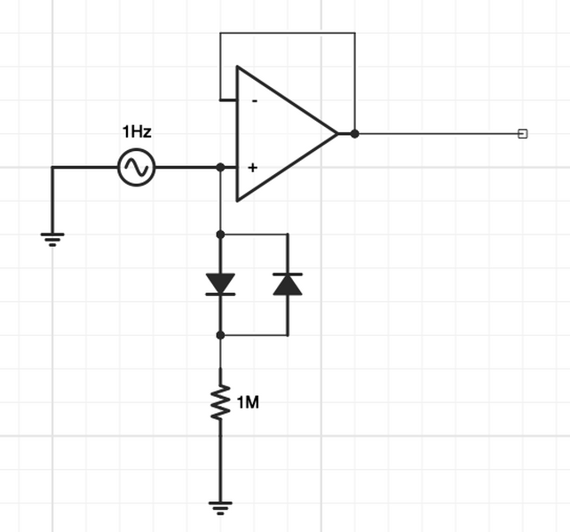
For those of you following along, here's the current experiment - which doesn't look very exciting I'll grant you. The signal generator shown here is where I have the capsule (an Ali Express special) mounted.
While not exciting, it's proven that you can use a couple of diodes in opposing polarities as a very (and I mean VERY) high impedance indeed. Some current does flow in this circuit but most of the voltage is developed directly into the JFET input of the op-amp - I'm using a TL072 here, but for now, I've got it running with split supplies. An OPA1642 would provide better performance at a greatly increased cost (relatively speaking).
The everyday silicon rectifier diodes are non-linear and appear to be non-functional (the forward voltage is usually 0.6 V) but we're using the fact that they conduct a very small amount and in combination with the 1M resistor form a very high impedance resulting in more signal delivered into the follower.
It's going to need some sort of bootstrap (which I haven't shown here because I haven't tested it) but that's just a capacitor connected from the output to where the two diodes meet the 1M resistor to "push" the diodes so the Vd remains roughly 0 - pushing the effective impedance into the stratosphere.
I've tested this small circuit with the external microphone input on a dictaphone and to my astonishment, it actually works rather well even without the bootstrap.
Interesting little experiment if you have a few minutes. Judging by the output level, I expect it won't need a x1000 (60 dB) amplifier to push it to "line" level but we'll see, I'll report back when I know more but if anyone fancies a go, I'd be interested to know how you get on.
Take everything I say with a pinch of salt, I might be wrong and it's a very *expensive* way to learn!
@axy_david Sorry, that is a little confusing. If you want the short answer, it's right down at the bottom but I've written up what I understand so it might help you if you're interested.
This is another long post with some fundamentals but hopefully it will clear stuff up.
It's a development from the OPA Alice design which offers (in theory) even higher performance from the capsule with very low distortion. This might be a little clearer as it's from the OPA Alice front end.
Figure 1
Although mine is drawn the other way up, you can see that 100% of the output from the op-amp is returned to the inverting input. This is a basic, ultra-high impedance configuration when used with any voltage-based op-amp (which is most of them). It's called a "follower" because the voltage on the output "follows" (is a match) for the voltage at the input.
So what?
The impedance at the output is very low which means it can drive a low-impedance stage further down the chain. It's a driver - or an interface if you prefer - between the very high impedance of the capsule and the relatively low impedance of a power amplifier. That's the THAT1512 in Matt's case or a balanced cable which might terminate at a 600-2K ohm input on a commercial mic pre-amp.
Ideally, each stage should have an output impedance of at least 10x the impedance of the preceding one (at signal frequencies) so we don't lose a lot of what we're after. The more we lose, the more we have to amplify and that means the more noise we end up with; and we don't want lots of noise!
This applies especially to the input from the sensor (the JLI2555 mic capsule in this case). We know that condensers present eye-wateringly high impedances to whatever is trying to drive them - they are, after all, very small capacitors so they block all DC (infinite impedance).
If you look on a typical data sheet you might see this quoted as 2K2 which doesn't seem all that much but that's the impedance AFTER a JFET has been added. It's the typical impedance of a common source amplifier we see in very small electrets that come with an internal FET and drive a (wait for it...) 2K2 load resistor. The internal FET is wired so its drain appears at the +ve input an the source is internally wired to the -ve terminal, the gate is wired to the capsule output.
Primo and others do make SDCs with internal FETs that have both the source and drain terminals available for special applications. Phase splitting would be typical but that requires more external circuitry to buffer the different output impedance at the source and the drain. Understanding that little nugget requires a bit more understanding of how JFETs are biased and that's beyond where we are here.
About Impedance
Impedances can be tricky to understand so I like to think of them as steering current. Current flow will divide itself according to Ohm's law through all the impedances (you can think of pure resistance here) presented to it.
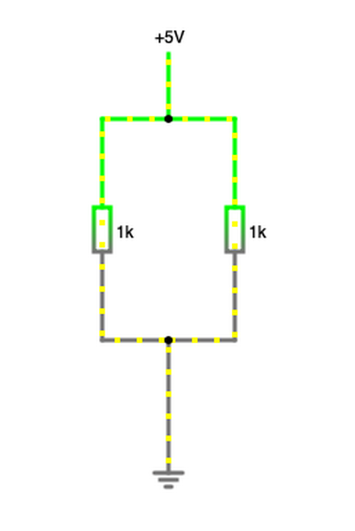
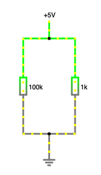
So if you have two equal value resistors in parallel that presents an impedance of 1/2 the value of either one. Nice and easy.
Figure 2
The total impedance in this circuit is 500 ohms so from Ohm's law we get 5V/500 = 10 mA. Kirchoff's first law states that the sum of all currents into a circuit must equal the total current at its output. Which seems blindingly obvious to me and a very complicated way of putting it. Teachers usually illustrate this with a huge, overly complicated network of resistors and wires and even voltage sources. But it's really just the same as rolling coins down those things we use to have in amusement arcades. What goes in MUST come out.
In this simple example, the current splits between the two resistors with 5 mA going through each which means that each one "drops" (another term I personally hate) 5 mA * 500 ohms = 2.5 V.
Now it might just be me, but "drops" always sounds bad. I don't want my voltage to DROP I want it to increase, right? I prefer the term "develops across" as it's clearer for what's going on but use whatever you're comfortable with.
Figure 3
Total voltage drop across this network is still 5V but with a bit of Ohm's law you'll see that the currents vary dramatically with almost everything being "robbed" by the 1K. The voltage across each is still 2.5V but the currents vary dramatically - and most of it is going through that 1K - which is where the majority of the signal information is flowing.
About Capacitance
So let's look at an electret condenser. It's roughly equal to a capacitor of around 50-100 pico-farads (I got that wrong in an earlier post) and it's got a fixed amount of charge.
If you're up on the basics of capacitors you'll know they store energy by retaining charge and normally we charge and discharge them through circuit designs like oscillators and filters. We use them to block DC because they are an insulator with a metal plate at either side. (If you think on that for a moment you'll make the horrible realisation that capacitors are everywhere... we call this stray capacitance but it's usually far too small to worry about). A small air gap between two bits of wire is a capacitor - albeit tiny, probably in the femto-farads. These things are only a problem at UHF and beyond so we don't need to worry.
Charge is measured in Coulombs but all you really need to know is that the larger the capacitor is, the more energy it can store and by extension a 50 pF capacitor can't store very much at all.
When we change the distance between the plates of a capacitor we also alter its value slightly. While you can't do this with a fixed capacitor without damaging it but on a condenser microphone we literally do exactly that.
So if the amount of charge that capacitor holds is determined by the distance between the plates, altering the distance means its ability to hold charge also changes. Charge is really just a bunch of electrons "stuck" to one plate because they are attracted to the positively charged molecules on the opposite plate. (The energy we put into a capacitor is what causes this effect to happen. Pulling free electrons from one conductor and letting them get stuck to the other one.)
This is very much like what happens when you rub your bonce with a balloon. You gather electrons on the balloon just like a capacitor does. Your hair is slightly more positively charged and is attracted to the balloon. Of course, you have to have hair to do that so that's me jiggered.
Clever stuff but really quite simple when looked at through this model (electrolytics work using a chemical process but most small capacitors do just this.
So what's really happening in a condenser microphone (and why the earlier and still the best need to be "charged" to work) is that as the distance between the plates changes, electrons are pushed and pulled to and from the plate.
That's what we are amplifying and that's an audio signal.
These features (and the delicate diaphragm) are what makes condenser microphones so incredibly sensitive with extremely low self-noise.
But here's where it gets a bit tricky.
The amount of charge entering/leaving a capacitor is measured in amperes per second (that's the Coulomb) - or 6.241509×10^18 electrons in one second for a 1 farad capacitor.
But a picofarad is only 1 x 10^12 of a farad and 50 pf so that (if my math is correct) means - roughly 6.24 x 50x10^6 electrons which means the amount of available charge that could flow is tiny (microamps). A tiny amount of charge (charge represents the static electrons) means that only a tiny amount of current can flow. If you know the potential charge on the plate, you can come up with the impedance and while it's impractical to measure this with everyday equipment you can assume it's in the order of 100s of megohms.
This is where that dratted load impedance comes in to effect.
Figure 4
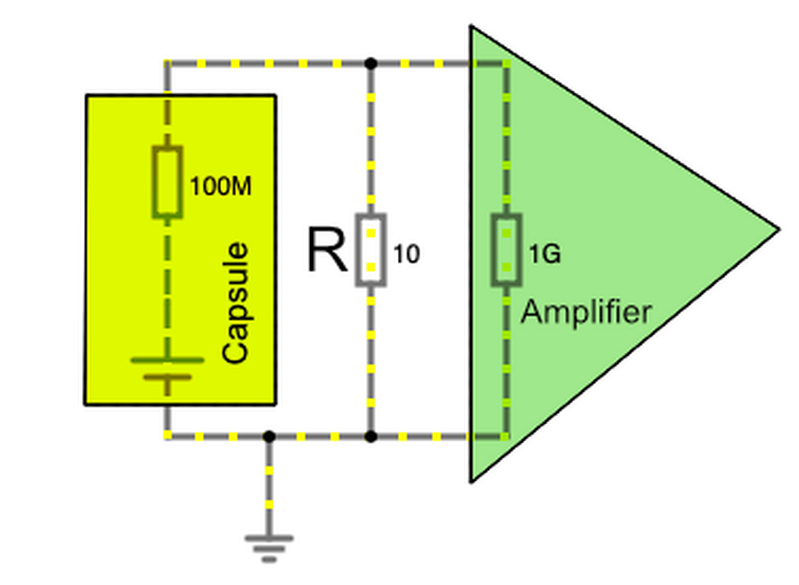
I've drawn a simplified version of an electret capsule here in the yellow with the amplifier in green. (You can see why I failed tech drawing...)
The capsule "looks" like a voltage source in series with a large resistor. (As an aside, you'll also see this listed in discussions of batteries where it's called the "internal resistance". In both cases, it's not really a resistance in terms of a physical thing, it's the ability of the "black box" (or yellow here) to deliver current. As a battery runs down we say it's internal resistance increases because as it discharges the amount of current it can provide into a given load drops off. The charge on our little electret won't vanish if you short it (as would happen with a normal capacitor) because it's "stuck" by some clever physics but it can push electrons around and this is where the internal impedance lies.
FETs have very high input impedances - they are voltage-to-current devices (transconductance) compared to bipolar transistors which are current driven, but I won't trouble you with another aside into that, you can just take that as read.
FETS and Robbers
OK so we've established that when you put resistors in parallel the smaller resistor "robs" most of the current (figure 3) and anything connected to that has to make do with the scraps: and that's the input to our amplifier (or even a discrete JFET). So the smaller the "load" resistor is in relation to the capsule's input impedance the more of that lovely signal gets INTO our amplifier and, eventually our ears.
The usual way to solve this is to stick a very high value resistor, 1G typically, into the load so the more current is available to drive the next stage. To small and we're loading the capsule - thus reducing the output.
It's not clear where this impedance is on the original Alice design but it's not usually good practise because impedances created as an effect of semiconductor leakages are non-linear and cause distortion.
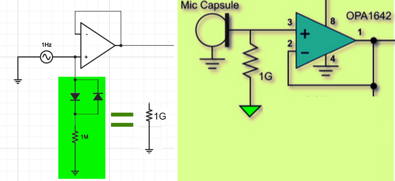
So if you're following along here you're probably wondering what the hell I'm doing using semiconductors (diodes) where the 1G load resistor goes! After all, I've just said these things are terribly non-linear.
While this is true, at very voltages and therefore low currents (and we're talking pico-amperes here) the distortion is very low (more of that shortly). The diodes don't turn "on" fully until the voltage across them hits around 0.6v and a capsule is unlikely to produce that much and will probably self-clip long before this circuit starts conducting.
So we've got fractions of picoamp flowing a potential difference (voltage) of say 1/10th of a volt - that puts the effective impedance in the 100s of GIGAohms loading the capsule.
In effect, you have an extremely high value (but non-linear) resistor.
The 1M is there for a later development called bootstrapping which I'm going to hook up today. Always assuming I've read the books correctly (cough, cough) this means passing a small amount of low-impedance output signal back to the 1M resistor. Since the output is "following" the input this pushes the bottom end of the two diodes to the same potential they "see" at the top end which linearises them. (As Doug Ford puts it, "bootstrap the buggers!").
The CIA used a device for their bugs that had these diodes on the die which means they were more predictable than what I've used here for experiment but it so far, I've been unable to detect significant distortion even without the bootstrap.
TL;DR
The circuit shown above replaces a very expensive (and potentially noisy) large value resistor with two diodes and a resistor.
Take everything I say with a pinch of salt, I might be wrong and it's a very *expensive* way to learn!

